Showing posts with label Basic Electronics. Show all posts

Monday, 23 December 2013

How P-N Junction Diode Is Work In Reverse Biasing ?

When the P-region or Anode of the diode is connected to the negative terminal of the external DC source and N-region or Cathode of the diode is connected to the positive terminal of the external DC source. At that time we can say that the Diode is in "Reverse Biased" condition.

The Reverse Biased condition is indicated in the Fig.15a.


                                                         Fig.15a

When a diode is reverse biased, holes in the p-regions are attracted towards the negative terminal of the external DC supply and electrons in the n-regions are attracted towards the positive terminal of the external DC supply.

Due to movements of electrons and holes away from the junction, "the width of the depletion region increases". This happens due to the creation of the more numbers of immobile ions.

Due to more numbers of immobile ions opposite the junction, "the barrier potential will increase".

We know that the p-region consists of a small number of electrons and n-region consists of a small number of holes. These minority charge carriers get some thermal energy and crossed the junction and produce some current.

This current is know as "Reverse Saturation Current" Which indicated in Fig.15b.


                                                         Fig.15b

 
The End.


How P-N Junction Diode Is Work In Forward Biasing ?

When the P-region or Anode of the diode is connected to the positive terminal of the external DC source and N-region or Cathode of the diode is connected to the negative terminal of the external DC source. At that time we can say that the Diode is in "Forward Biased" condition.

The Forward Biased condition is indicated in the Fig.14a.


                                                               Fig.14a

When the Diode is in Forward biased condition, the free electrons from n-side are pushed towards the p-side. Similarly the holes from p-sides are pushed towards the n-side.

With increase in the external supply voltage V, more and more number of holes and electrons start traveling towards the junction.

Thus the holes will start converting the negative ions into the neutral atoms and the electrons will start converting the positive ions into the neutral atoms. Therefore we can say that "the width of the Depletion Layer or Region will reduce".

Due to reduction in the depletion region width, the barrier potential will also reduce. Then At a particular value of V the Depletion region will collapse. There are no traveling of holes and electrons.


                                                             Fig.14b

The large number of majority carrier crossing the junction produces a current called as the "Forward Current" which indicated in the Fig.14b.

The End.


Also look out;

Post-15 How P-N Junction Diode Is Work In Reverse Biasing ?

Post-13 Biasing Of A P-N Junction Diode(With External Bias)


God Bless Thx.....

Biasing Of A P-N Junction Diode (With External Bias)

When the P-N Junction is formed, the depletion region gets created and movement of electrons and holes stops. Thus the current flowing through an unbiased P-N Junction is zero.

To make current to flow we have to Bias the P-N Junction Diode. Biasing is the process of applying external DC voltage to the semiconductor diode.

When the external voltage is not applied to the diode, the P-N Junction will remain in the state of equilibrium. Therefore there is no current flowing through it.

To make the current to flow, it is necessary to "Bias" the diode. The biasing can be two types;

[1] Forward Bias

To know how diode work in this condition, visit below post;

Post-14 How P-N Junction Diode Is Work In Forward Biasing ?

[2] Reverse Bias

To know how diode work in this condition, visit below post;

Post-15 How P-N Junction Diode Is Work In Reverse Biasing ?


Also look out below post;

Post-8 Formation of P-N Junction Diode(Without External Bias)


God Bless Thx.....

Thursday, 19 December 2013

Formation of P-N Junction Diode(Without External Bias)

Go through that;
 

Post-6 N-type Semiconductor's structure and electric conduction


By reading above two posts you understand that how P-type and N-type extrinsic semiconductor works. After that we will make the P-N Junction diode.......How..?

Let's see....

When we join the P-type semiconductor to the N-type semiconductor permanently we will get P-N Junction Diode which is shown in Fig.8a.


                                                     Fig.8a

We earlier see that N-type semiconductor consists more number of the free electrons than the P-type semiconductor, there fore "Diffusion" will occurs. 


It means that the free electrons of N-type moves towards the P-type and fill the empty place in the P-type. And also we can say that the less number of holes moves towards the P-type to N-type. 

These conditions shows in the Fig.8b.


                                                   Fig.8b

After that situation, at the junction P-type contains more number of aluminum ions and N-type contains more number of Arsenic ions it means that P-type and N-type consists negative and positive charge respectively.

For these charges, The electric field creates at the junction from N-type to P-type it means N-type having positive potential and P-type having negative potential. But the total potential become zero at the junction.

After that now the free electrons want to pass the junction it face the electric field which creates from N-type to P-type. 


When the electric field become more powerful, the diffusion of electrons-holes will stop which shows in Fig.8c.


                                                        Fig.8c

By these process we can conclude two major things which are as follows;

[1] Junction contain two small N-type and P-type place which are not contain there majority carrier as electrons and as holes respectively. this place at the junction is known "Depletion Layer". The breadth of the depletion layer is 0.5 um.

[2] The Electric Potential creates in the depletion layer is known as "Depletion Barrier". Here it is 0.1 volts.

Note:-The Depletion Barrier and Depletion Layer in P-N Junction Diode depends upon the impurities added in to the P-type and N-type semiconductor.

Impurities less=Depletion Layer increase=Electric Field become weak 
 

Impurities more=Depletion Layer decrease=Electric Field become high


God Bless Thx...... 

Wednesday, 18 December 2013

P-type Semiconductor's Structure and Electric Conduction

We all know that the material which is semiconductor having two types which follows as
           [1] intrinsic semiconductor and
           [2] extrinsic semiconductor.

For the understanding of intrinsic type semiconductor please visit below post;
 
Post-3 How Silicon or Germanium is working as an Semiconductor ?
 

For the understanding of extrinsic donor semiconductor please visit below post;
 
Post-6 N-type Semiconductor's Structure and Electric Conduction

Now we come to the point and explain that what is the extrinsic acceptor semiconductor type; what is the meaning of 'P'; and what is the structure and its electric conduction.

First note that when we add any impurities in the intrinsic material then after these material becomes 'Extrinsic material' and the process of adding impurities is called "Doping".

Ex. Tetra-valent silicon will contain tri-valent impurities which are aluminum, Gallium and Indium.

As shown in Fig.7a, when a Gallium atom is added to the silicon lattice, there are three valence electrons will construct three co-valent bonds with the valence electrons of three neighboring silicon atoms.
 

                                                  Fig.7a
 
The fourth co-valent bond consists one valence electron but that place remains empty and create 'hole' represented by a small circle in Fig.7a.

A hole is positively charged as it represents the absence of a negative charge. thus because each tri-valent impurity atom added, a hole is created which always attract electron for its empty place circle. this type is called extrinsic acceptor impurities which shown in Fig.7b.


Fig.7b

If we notice for whole lattice, there are more number of holes are established in the P-type semiconductor. And it is possible to control the number of holes by controlling the 'Doping Concentration'.

A large number of holes are present along with a small number of thermally generated electrons in a P-type semiconductor material. That's why the holes are called "Majority charge carrier" and the electrons are called "Minority charge carrier".


                                                  Fig.7c
 
Then after we talk about electric conduction, when an external DC voltage is applied to the P-type semiconductor material, the holes(called Majority charge carrier) move towards to the negative terminal of the battery and the electrons(called Minority charge carrier) move towards the positive terminal of the battery which indicated in Fig.7c.


God Bless Thx......

N-type Semiconductor's Structure and Electric Conduction

We all know that the material which is semiconductor having two types which follows as
           [1] intrinsic semiconductor and
           [2] extrinsic semiconductor.

For the understanding of intrinsic type semiconductor please visit below post;
 
Post-3 How Silicon or Germanium is working as an Semiconductor ?

Now we come to the point and explain that what is the extrinsic donor semiconductor type; what is the meaning of 'N'; and what is the structure and its electric conduction.

First note that when we add any impurities in the intrinsic material then after these material becomes 'Extrinsic material' and the process of adding impurities is called "Doping".

Ex. Tetra-valent silicon will contain penta-valent impurities which are Phosphorus, Antimony and Arsenic.

The penta-valent element is the one which has five valence electrons and after add in the silicon base what effect is generated is shown in Fig.6a.
 

                                                            Fig.6a

When a penta-valent impurity such as Arsenic is added to the intrinsic semiconductor, four valence electrons of Arsenic atom construct four co-valent bonds with the four neighboring Silicon atoms as shown in Fig.6a.

The fifth electron of the Arsenic atom does not construct any co-valent bond with other and act as a free electron in the lattice-structure and take part in the electric conduction.

At the room temperature Si gets 0.01ev thermal energy and donate extra electron to the base silicon. that's why these type of impurities called "Donor impurities" Which indicated in Fig.6b.

                                                                            Fig.6b

The number of impurities electrons is one per 10^6 intrinsic atoms. It means that one mole lattice consists of 10^17 impurities electrons.

As a reason that A large number of free electrons are present along with a small number of thermally generated holes in an N-type semiconductor.

So the conduction largely takes place due to the free electrons. There fore the free electrons are called as "Majority Carriers" and holes are called as "Minority Carriers".
 

                                                                   Fig.6c

Then after we talk about electric conduction, when an external DC voltage is applied to the N-type semiconductor material, the free electrons(called Majority charge carrier) move towards the positive terminal of the battery and holes(called Minority charge carrier) move towards to the negative terminal of the battery which indicated in Fig.6c.


For P-type semiconductor material wait to the next post.........

Post-7 P-type Semiconductor's Structure and Electric Conduction


God Bless Thx......
 

Tuesday, 17 December 2013

How Silicon or Germanium is working as an Semiconductor ?

The electric conditions of any elements can be depend on its lattice-structure and the electrons shells structure. Here we learn two famous semiconductor Si and Ge which have Diamond lattice-structure. The schematic of the Silicon is shown in Fig.3a.

 
    Fig.3a.

Si(and Ge) is a tetravalent because silicon's electric structure is 1s2 2s2 2p6 3s2 3p2. If we recall that K and L shells of Si is fully complete because of 1s2 2s2 2p6. Thus the remaining 3s2 3p2 contains valence electrons. Then after two s states and two p states create sp3 shells.

These shells joins with the neighboring shells and create co-valent bond. If say in simple the atom contains four valence electron and it creates four co-valent bond with the four neighbor atoms valence electrons which shows in Fig.3b.
 
 
    Fig.3b.

The electrons which in co-valent bond stay static at 0K temperature. Thus reacts as an insulators.

At room temperature, crystal atom contains thermal oscillations. For thus reason some co-valent bond breaks and electron is now a free electron and participating in electric current. Some positive charge create at the place of free electron and it try to catch the other free electron at that place. This empty place is called "Hole".

At these situation we will provide Potential Differene between crystal two ends, the free electrons travels negative side to positive side of battery and produce electric current which shows in Fig.3c.


                                                               Fig.3c.

Under effect of the thermal oscillation and external electric field, other free electrons break the co-valent bond and jump in to the hole and creats new holes. For these formation we can say that electrons travels negative sides to positive sides and holes travels positive sides to negative sides.

Thus, Two types of electric current flow in the semiconductor which are as
[1] the motion of free electrons
[2] the motion of free electrons which jumps into the empty holes

Semiconductors have ne and nh which follows free electrons and holes respectively but in intrinsic semiconductor it is equal and it is expressed with ni.
                                                       

                                                            ne=nh=ni

 
Also visits other Post;

Post-2 The Energy-Band Theory of Crystals


God Bless Thx....

The Energy-Band Theory of Crystals

A crystal consists of a space array of atoms or molecules built up by regular repetition in three dimensions of some fundamental structural unit. The electronic energy level for single free atom do not apply to the same atom in a crystal.

When atoms form crystals, it is found that the energy levels of the inner-shell electrons are not affected by the presence of the neighboring atoms. However the levels of the outer-shell electrons are changed and these electrons are shared by more than one atom in the crystal.

A brief discussion of the energy band structure of one element which consisting of N atoms shows below.


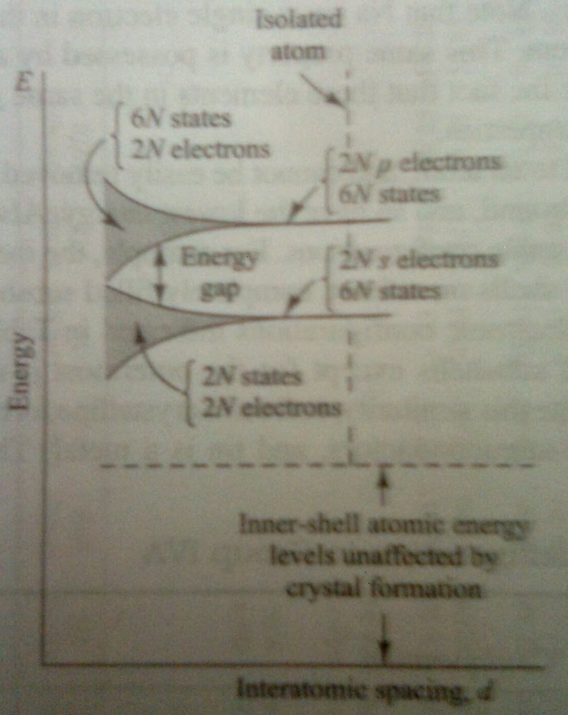
Fig.2
 
Imagine that it is possible to vary the spacing between atoms without altering the type of fundamental crystal structure. If the atoms are so far apart that the interaction between them is negligible, the energy levels will coincide with those of the isolated atoms. 

For the taken element the outer two subshells contains 2 s electrons and 2 p electrons. Indicated to the extreme right in fig.1a, there are 2N electrons completely filling the 2N possible s levels. all at the same energy level. Since the p atomic subshells has 6 possible states which fill only 1/3rd of the 6N possible p states, all at the same energy level. 

 
Fig.2a

If we now decrease the interatomic spacing of our imaginary crystal(moving right to left in Fig.2a), an atom will exert an electric force on its neighbors.

Hence, the 2N degenerate s states must spread out in energy. The separation between levels is small, but since N is very large, the total spread betweenthe minimum and maximum energy may be several electrons volts if the interatomic distance is decreased sufficiently. This large number of discrete but closely spaced energy levels is called an "Energy Band" and indicated by the shaded region in Fig.2a.

In Fig.2b, small enough distances these bands will overlap. Under such conditions the 6N upper states merge with the 2N lower states, giving a total of 8N levels, half of which are occupied by the 2N + 2N = 4N available electrons.
 
Fig.2b

At this spacing each atom has given up four electrons to the band, these electrons can no longer be said to orbit in s or p subshells of an isolated atom, but rather they belong to the crystal as a whole. In this sense taken element is tetravalent, since they contribute four electrons each to the crystal. The band these electrons occupy is called the "Valence Band".

If the spacing between atoms is decreased below the distance at which the bands overlap, the interaction between atoms is indeed large. At the crystal-lattice spacing, we find the valence band filled with 4N electrons separated by a forbidden band of extent Eg from an empty band consisting of 4N additional states. This upper band is called the "Conduction Band".


God Bless Thx.......   


Monday, 16 December 2013

Insulators, Semiconductors and Metals

A very poor conductor of electricity is called an insulators; an excellent conductor is a metal; and a substance whose conductivity lies between these extremes is a semiconductor. A material may be placed in one of these three classes, depending upon its energy-band structure.


Insulators
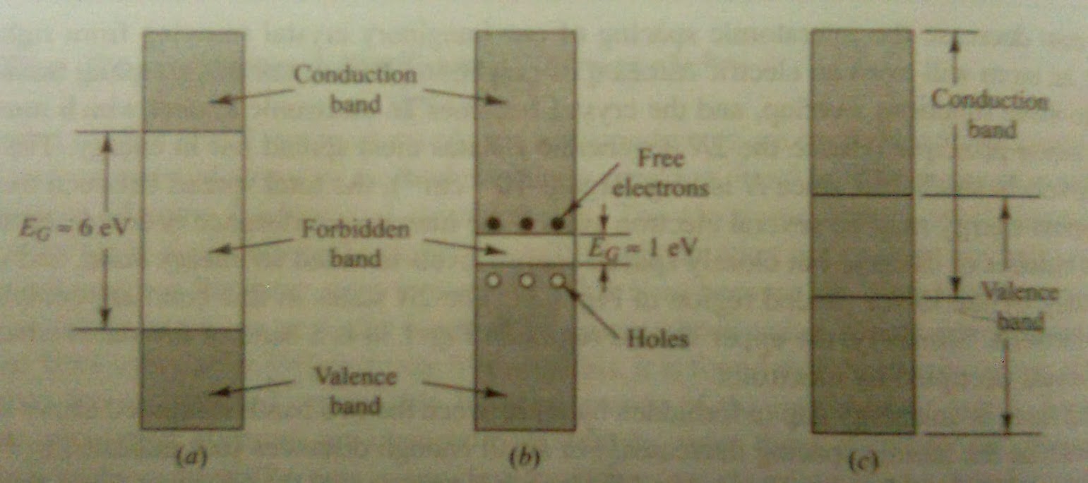
The energy band structure of insulator is indicated in schematically in Fig.1 (left side). 
For a diamond crystal the region containing no quantum states is several electron volts high(6ev). 
This large forbidden band separates the filled valence region from the vacant conduction band. 
The energy which can be supplied to an electron from an applied field is too small to carry the particle from the filled into the vacant band. 
Since the electron can't acquire sufficient energy, conduction is impossible, and hence diamond is an insulator. 

Semiconductor
A substance for which the width of the forbidden energy region is relatively small(1ev) is called semiconductor.
Graphite, a crystalline form of carbon but having a crystal symmetry which is different from diamond, has such a small value of Eg, and it is a semiconductor.
As the temperature is increased, some of these valence electrons acquire thermal energy greater than Eg, and hence move into the conduction band. 
These are now free electrons in the sense that they can move about under the influence of even a small applied field.
These free or conduction electrons are indicated in Fig.1(Middle) and the insulator has now become slightly conducting; it is semiconductor.

Metal
A solid which contains a partly filled band structure is called a metal. Under the influence of an applied electric field the electrons may acquire additional energy and move into higher states. 
Since these mobile electrons constitute a current, this substance is a conductor and the partly filled region is the conduction band.
One example of the band structure of a metal is given in Fig.1(right side) which shows overlapping valence and conduction bands. 


God Bless Thx...